Abstract
In a global context characterized by steadily rising energy demand, dwindling fossil fuel resources, and escalating environmental concerns, the transition to clean, sustainable alternative energy sources is critical. This study addresses this challenge by numerically simulating the performance of an amorphous silicon-based (a-Si) solar cell, aiming to optimize the thickness of the i(a-Si(p): H) absorber layer and the operating temperature to achieve a highly efficient and stable photovoltaic structure. To this end, a Substrat/Right contact (ZnO)/a-Si(p)/i-a-Si(P)/a-Si(n)/Left contact configuration was modeled and simulated using the Solar Cell Capacitance Simulator-1D (SCAPS-1D) software. The numerical results demonstrate that increasing the thickness of the i(a-Si(p): H) layer enhances all photovoltaic electrical parameters. Conversely, with the exception of the short-circuit current density, these parameters degrade as the operating temperature rises. This indicates that a thicker absorber layer ameliorates the absorption of incident photons, effectively converting them into electron-hole pairs and collected at the contacts. Whereas elevated temperatures accelerate carrier recombination within the space-charge region. Under optimized conditions an absorber thickness of 5000 nm at an operating temperature of 300 K, the device achieves an open-circuit voltage of 0.94 V, a short-circuit current density of 32.30 mA/cm2, a fill factor of 86.88%, and a power conversion efficiency (η) of 26.41%. With the aim of developing stable, high-performance, lightweight, and high-efficiency a-Si(H)-based PV solar cells, we have selected an absorber layer thickness of 2.5 µm, an energy gap of 1.72 eV, and an operating temperature of 300 K. Under these conditions, we obtain the following electrical parameters: VOC=1.21 V, JSC= 20.14 mA/cm2, FF= 86.94%, η= 21.17%. In future studies, we will investigate the effects of electron affinity and bandgap variations within the i(a-Si(p): H) absorber layer.
Keywords
PV Solar Cell, Amorphous Silicon, Absorber Layer, Temperature, Electrical Parameters, SCAPS-1D
1. Introduction
Driven by steadily rising global energy demand, diminishing fossil fuel reserves, and mounting environmental concerns, the transition toward clean and sustainable alternative energy sources has become an urgent imperative
| [1] | Hüseyin Çelik, Mumtaz Ali, Muhammad Adeel, et al. (2024). Towards a carbon-free society: Innovations in green energy for a sustainable future. Journal of Minerals, Metals and Materials Society (24(5): 103121.
https://doi.org/10.1016/j.rineng.2024.103121 |
[1]
. Consequently, investments from funding institutions and research efforts within the scientific community are accelerating rapidly in the renewable energy sector, particularly in solar photovoltaics (PV)
| [2] | IRENA. (2023). World Energy Transitions Outlook 2023: 1.5°C Pathway [Vol. 1]. International Renewable Energy Agency. Abu Dhabi.
https://www.irena.org/Publications/2023/Jun/World-Energy-Transitions-Outlook-2023 |
| [3] | Khan, Z., et al. (2023). Transitioning to clean energy: Assessing the impact of renewable energy, bio-capacity and access to clean fuel on carbon emissions in OECD economies. Energy Economics, 127, Article 107091. doi.org |
[2, 3]
. The primary technological challenge today is to develop devices that merge low production costs, high conversion efficiency, exceptional long-term stability, and scalability for mass manufacturing to guarantee universal access
| [1] | Hüseyin Çelik, Mumtaz Ali, Muhammad Adeel, et al. (2024). Towards a carbon-free society: Innovations in green energy for a sustainable future. Journal of Minerals, Metals and Materials Society (24(5): 103121.
https://doi.org/10.1016/j.rineng.2024.103121 |
| [2] | IRENA. (2023). World Energy Transitions Outlook 2023: 1.5°C Pathway [Vol. 1]. International Renewable Energy Agency. Abu Dhabi.
https://www.irena.org/Publications/2023/Jun/World-Energy-Transitions-Outlook-2023 |
| [3] | Khan, Z., et al. (2023). Transitioning to clean energy: Assessing the impact of renewable energy, bio-capacity and access to clean fuel on carbon emissions in OECD economies. Energy Economics, 127, Article 107091. doi.org |
[1-3]
.
For decades, silicon has served as the baseline material for solar cell manufacturing due to its natural abundance, non-toxicity, and favorable optoelectronic properties. However, despite their high efficiency, crystalline silicon PV cells suffer from notable drawbacks: elevated production costs and structural rigidity that limit their deployment in emerging, flexible applications.
To bypass these limitations and engineer PV cells that are both economical and high-performing, amorphous silicon (a-Si): H has emerged as a first plan alternative, fueling intense interest across the scientific community. Distinguished by unique physical properties, amorphous silicon enables the fabrication of thin-film solar cells that are flexible, cost-effective, and readily integrated into diverse structural surfaces
| [4] | Md. Nazmul Islam Sarkar et H. R. Ghosh (2017). Efficiency improvement of amorphous silicon single junction solar cell by design optimization. International Conference on Electrical, Computer and Communication Engineering (ECCE) (Cox's Bazar, Bangladesh).
https://doi.org/10.1109/ECACE.2017.7912989 |
| [5] | Teyou Ngoupo et al., “Numerical Design of Ultra-Thin Hydrogenated Amorphous Silicon Solar Cells,” 2021. Street, R. A. (1991). Hydrogenated Amorphous Silicon. Cambridge University Press. https://doi.org/10.1017/CBO9780511525247 |
[4, 5]
. Even so, the conversion efficiency of these amorphous silicon devices remains constrained by a high concentration of structural defects inherent to its disordered atomic network
| [6] | J. de Kordesch, M. A. Flores, L. N. Martínez, E. R. Silva, et T. O. Santos (2024). Inherent structural defects and atomic disorder limitations on the conversion efficiency of amorphous silicon photovoltaic devices. Journal of Non-Crystalline Solids.
https://doi.org/10.1016/j.jnoncrysol.2024.12284 |
[6]
.
This study aim to optimize the performance of an amorphous silicon-based photovoltaic solar cell by systematically evaluating the impacts of absorber layer thickness and operating temperature to design a structure that balances high efficiency with long-term stability. To achieve this, we first outline the theoretical model and simulation methodology developed for our specific Substrat/Right contact (ZnO)/a-Si(p)/i-a-Si(P)/a-Si(n)/Left contact architecture. We then present and analyze the resulting current density-voltage (J-V) characteristics and quantum efficiency (QE) profiles to determine the optimal configuration.
2. Materials and Method
2.1. The SCAPS Simulation Tool
Developed at Ghent University in Belgium by Marc Burgelman and his team
| [7] | Cheick Sid El Moctar Salamata, “Study and AC simulation of the electrical characteristics of some thin film solar cells”. Ibn-Khaldoun University of Tiaret, Tiaret, Algeria (2019). |
[7]
, SCAPS (Solar Cell Capacitance Simulator) is a free, user-friendly, one-dimensional software designed to model photovoltaic solar cells. While initially created for thin-film devices like CdTe and CuInSe
2 , the program has since expanded to support other technologies, including crystalline silicon, gallium arsenide, and amorphous structures. It can handle up to seven distinct semiconductor layers alongside front and back contacts. Organized through intuitive configuration panels, SCAPS delivers precise outputs such as dark and illuminated current density-voltage (J-V) curves
, capacitance-voltage and capacitance-frequency profiles, and spectral responses
. Its high accuracy stems from numerically solving foundational semiconductor charge-transport equations, specifically Poisson's equation and the continuity equations for both electrons and holes. These robust capabilities establish SCAPS-1D as an essential benchmark for optimizing photovoltaic performance, which explains why it attracted our interest.
2.2. Structure of the a-Si-based PV Solar Cell Model
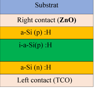
A simplified diagram of the structure of this PV solar cell is shown in
Figure 1.
Figure 1. Structure of the a-Si PV solar cell.

The role of each layer of this solar PV structure is to:
1) Substrate / Front contact: This layer serves as the physical base for the cell and collects electric charges. The front contact is generally composed of a transparent conductive oxide (TCO) such as ZnO. It must be highly transparent to allow maximum light transmission while acting as an excellent electrical conductor to transport holes or electrons to the external circuit
| [10] | J. Poortmans et V. Arkhipov (2006). Thin Film Solar Cells: Fabrication, Characterization and Applications. Edited by Jef Poortmans and Vladimir Arkhipov IMEC, Leuven, Belgium. |
[10]
.
2) p-layer (p-doped a-Si: H): This layer is enriched with holes through doping, often with boron. Its primary role is to create a strong internal electric field by pairing with the n-layer on the opposite side of the intrinsic layer
| [11] | J. Nelson. The Physics of Solar Cells. London, UK: Imperial College Press, 2003. P. 363 à 384. |
[11]
. It also assists in collecting light-generated holes but must remain very thin to avoid blocking or unnecessarily absorbing photons before they reach the active zone
| [12] | R. A. Street, Hydrogenated Amorphous Silicon. Cambridge, UK: Cambridge University Press, 1991. |
[12]
.
3) i-layer (intrinsic a-Si: H): This is the cell active and thickest layer, composed of pure (undoped) amorphous silicon. It is within this layer that incident photons from the light are absorbed, releasing electron-hole pairs
. Subjected to the strong electric field created by the adjacent doped layers, this layer effectively separates these charges and propels them toward their respective contacts before recombination occurs
| [14] | J. Zhang, L. Wang, H. Liu, and X. Tan. (2026). Transparent Conductive Oxide Electrodes in Perovskite Solar Cells: Optical and Electrical Optimization. Chemistry Europe.
https://doi.org/10.1002/cssc.202502745 |
[14]
.
4) n-layer (n-doped a-Si: H): This layer is enriched with electrons through doping, typically with phosphorus. Together with the p-layer, it establishes the p-i-n junction and the cell overall electric field. It serves as a collection and transport zone for free electrons moving toward the cell back contact
.
5) Back Contact (Metal / TCO): This layer completes the electrical circuit at the back of the cell to collect electrons. Using a combination of TCO and aluminum not only ensures excellent electrical conductivity but also acts as an optical mirror, reflecting unabsorbed light back through the cell to increase its efficiency
| [15] | J. Mitra, A. Oudhia, S. Verma. (2025). Zinc Oxide in Solar Cells: A Comprehensive Review on Its Dual Role as an Emitter and Antireflection Layer Journal of The Minerals, Metals & Materials Society. Flight. 77, pp. 6535-6547.
https://doi.org/10.1007/s11837-025-07211-w |
| [16] | Min-Gu Kang, Tae-Won Kim, Kyu-Sun Song & Dong-Seob Kim. (2025). Design of the Front Electrode Patterns of Solar Cells Using Two-Dimensional Simulation. Applied Sciences.
https://doi.org/10.3390/app152011154 |
[15, 16]
.
2.3. Operating Principle
The operating principle of this solar PV structure relies on the conversion of light into electricity via an internal electric field
| [17] | Cherif, E. S., Lakhdar, N., Ziane, M. (2021). Numerical simulation and optimization of thin-film p-a-Si: H / n-a-Si: H buffer / p-c-Si heterojunction solar cells. Silicon, 13(10), 3467-3475. https://doi.org/10.1007/s12633-020-00827-0 |
[17]
. Incident photons pass through the front transparent contact and are primarily absorbed in the intrinsic (i) layer, generating electron-hole pairs. The strong internal electric field, created by the potential difference between the p-doped and n-doped layers, immediately separates these charges: holes are propelled toward the front contact (p-layer) and electrons toward the back contact (n-layer)
| [18] | Würfel, P. (2005). Physics of Solar Cells: From Principles to New Concepts. Wiley-VCH. ISBN printed: 9783527404285. ISBN online: 9783527618545.
https://doi.org/10.1002/9783527618545 |
[18]
. This flow of charges, collected by the metal and TCO (transparent conductive oxide) contacts, generates a direct electric current
| [19] | Sze, S. M., & Ng, K. K. (2006). Physics of Semiconductor Devices. John Wiley & Sons. (3e ed.), ISBN papier: 978-0-471-14323-9. ISBN electronic / O-Book: 978-0-470-06832-8.
https://doi.org/10.1002/0470068329 |
[19]
.
Table 1 shows the properties of the PV solar cell.
Table 1. Properties of the amorphous silicon-based PV solar cell.
Parameters | p-a-Si: H | n-a-Si: H | i-a-Si: H | ZnO |
W(nm) | 20 | 50 | 500-5000 | 150 |
Eg(eV) | 1.2 | 1.72 | 1.8 | 3,3 |
ᵡe(eV) | 4.1 | 3.8 | 3.9 | 4 |
ɛ/ɛ0 | 13,6 | 10 | 11.9 | 9 |
NC(cm-3) | 2.2x10¹⁸ | 2.2x10¹⁸ | 1020 | 2.2x10¹⁸ |
NV(cm-3) | 1.78x10¹⁹ | 1.78x10¹⁹ | 1020 | 1.78x10¹⁹ |
ʋe(cm/s) | 107 | 107 | 107 | 107 |
ʋh(cm/s) | 107 | 107 | 107 | 107 |
µe(cm2/Vs) | 102 | 102 | 20 | 102 |
µh(cm2/Vs) | 25 | 25 | 5 | 25 |
NA [cm-3] | 2x10¹⁶ | - | 1010 | - |
ND [cm-3] | - | 2x10¹⁸ | 105 | 1018 |
Nt | 3x10¹⁸ | 1018 | 2x10¹⁵ | 3x10¹⁴ |
Base parameters of a-Si: H cell properties. Eg—bandgap, χ
e —electron affinity, µ—mobility, N
A; N
D —dopant densities, W—layer thickness, N
V, N
C —effective density of states in the valence and conduction bands, ↋—relative permittivity, Nt—total defect density.
| [20] | Sawadogo, B. 2025. Analysis of the influence of the absorber layer and temperature on the amorphous silicon-based PV solar cell. Master thesis. Joseph Ki-Zerbo University, Ouagadougou, Burkina Faso. |
| [21] | Zhu, H., Kalkan, A. K., Hou, J., & Fonash, S. J. (1999). Applications of AMPS-1D for solar cell simulation. Flight 462 (1) pp. 309-314). AIP Conference Proceedings. |
| [22] | Ke Shaoying, Wang Chong, Pan Tao, Yang Jie, Yang Yu. (2014). Numerical simulation of the performance of the a-Si: H/a-SiGe: H/a-SiGe: H tandem solar cell.
https://doi.org/10.1088/1674-4926/35/3/034013 |
| [23] | Melis Bilgic Aksari, Aynur Eray. (2011). Optimization of a-Si: H/c-Si Heterojunction Solar Cells By Numerical Simulation. Energy Procedia. https://doi.org/10.1016/j.egypro.2011.10.160 |
[20-23]
.
3. Results and Discussion
3.1. Influence of the Absorber Layer Thickness i(p-a-Si: H)
In this section, we use an absorber band gap of 1.72 eV, a temperature of 300 K, and an illumination of 1000 W/m2.
3.1.1. Influence of Thickness on the J-V Characteristic
The curves of
Figure 2 show that the current density and voltage values of the PV solar cell increase as the thickness of the i(a-Si(p)) absorber layer increases. These results are attributed to enhanced absorption of incident radiation, which generates more charge carriers within the absorber layer.
Figure 2. J-V characteristic as a function of i(a-Si(p)): H thickness.
These results are consistent with the results found by Glunz et al. in 2012
| [24] | Glunz et al., IEEE Journal of Photovoltaics, 2(1), 95-101, 2012. |
[24]
.
To better understand the effects of absorber thickness, we examine its influence on various electrical parameters in the following sections.
3.1.2. Influence of the Absorber Layer Thickness on Electrical Parameters
From
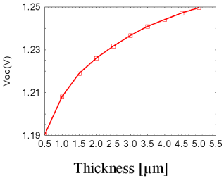
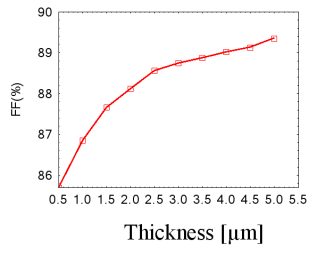
Figures 3-6, we observe that increasing the thickness of the absorber layer leads to an increase in the electrical characteristics (Voc, Jsc, FF, and η) of the simulated PV solar cell.
Figure 3. Variation of the open-circuit voltage as a function of the i(a-Si(p)) thickness.
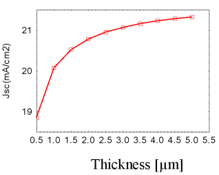
Figure 4. Variation of current density as a function of i(a-Si(p)) thickness.
The increase in Voc is attributed to the strengthening of the internal electric field and the reduction of recombination at the interface.
Furthermore, when the i(p-a-Si) layer is too thin, its doping level is insufficient to effectively pin the Fermi level on the p-side. Increasing the thickness enhances the space charge within the p-layer, thereby maximizing the structure built-in potential (Vbi).
The increase in Jsc values can be explained by improved photogeneration of incident photons within the i(p-a-Si) layer, followed by efficient collection of the resulting charge carriers at the contacts.
Figure 5. Variation of the fill factor as a function of i(a-Si(p)) thickness.
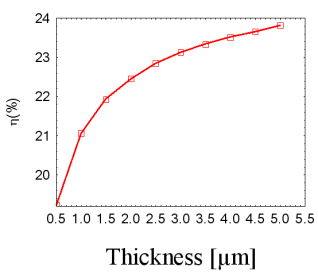
Figure 6. Variation of conversion efficiency as a function of i(a-Si(p)) thickness.

An increase in FF values reflects an improvement in junction quality and a reduction in electrical leakage.
This increase in FF may result from a reduction in shunt currents, leading to higher shunt resistance (RSh) values. Increasing the thickness yields a more uniform and continuous layer, thereby eliminating leakage currents.
The increase in Voc, Jsc, and FF in our solar PV structure is particularly pronounced for a-Si layer thicknesses between 0.5 µm and 3 µm, highlighting the need for an optimal thickness to achieve high performance and good stability.
3.2. Influence of Thickness on Quantum Efficiency (QE)
From
Figure 7, we observe enhanced QE performance between 400 nm and 700 nm, reaching 85% for thicknesses ranging from 3 µm to 5 µm. This trend is attributed to more efficient photon absorption at these wavelengths, enabling near-optimal electron-hole pair generation
| [25] | Bube, Photovoltaic Materials. Imperial College Press. ISBN-10. 186094065X ISBN-13. 978-1860940304. 1998. |
[25]
. Thinner layers (less than 2 µm) exhibit a drop in QE beyond 600 nm, reflecting optical losses due to the partial transmission of unabsorbed photons; this is confirmed by the work of Steven Hegedus et al.
| [26] | Antonio Luque, Steven Hegedus, Handbook of Photovoltaic Science and Engineering. Wiley. 2003. Print ISBN: 9780471491965; Online ISBN: 9780470014004. |
[26]
.
Figure 7. Quantum yield as a function of i(a-Si(p)) thickness.

Ultimately, we consider that increasing the thickness of the absorber layer indeed leads to increased absorption of incident photons, which accounts for the rise in Jsc values observed in Section 3.1.2.
3.3. Influence of Temperature on the J-V Characteristic
In this section, we use a thickness of 2.5 µm and a band gap of 1.72 eV of the absorber layer to achieve our goal of creating lightweight, high-performance solar cells with high efficiency, under an illumination of 1000 W/m2.
Figure 8 shows the current density-voltage (J-V) curves, and
Table 2 presents the electrical parameter values extracted from these curves for temperatures ranging from 280 K to 380 K. We observe that the open-circuit voltage decreases as the temperature rises. This result is explained by the increase in thermal recombination of minority carriers, which reduces the chemical potential difference between the conduction and valence bands
| [4] | Md. Nazmul Islam Sarkar et H. R. Ghosh (2017). Efficiency improvement of amorphous silicon single junction solar cell by design optimization. International Conference on Electrical, Computer and Communication Engineering (ECCE) (Cox's Bazar, Bangladesh).
https://doi.org/10.1109/ECACE.2017.7912989 |
[4]
. Conversely, increased photon absorption at longer wavelengths leads to deep charge-carrier generation, resulting in a very slight.
increase in short-circuit current
| [27] | Daouda Oubda, “Characterization of a CIGS-based thin-film cell as a function of the nature of the buffer layer,” 2018. PhD Thesis. Joseph Ki-Zerbo University, Ouagadougou, Burkina Faso. |
[27]
. Furthermore, the rise in the PV solar cell temperature causes expansion of the semiconductor material crystal lattice. The bandgap value decreases, leading to an increase in saturation current
| [27] | Daouda Oubda, “Characterization of a CIGS-based thin-film cell as a function of the nature of the buffer layer,” 2018. PhD Thesis. Joseph Ki-Zerbo University, Ouagadougou, Burkina Faso. |
[27]
.
Figure 8. J-V characteristic as a function of temperature.

In addition to Voc, electrical parameters such as the fill factor and conversion efficiency decrease with rising temperature (
Table 2) due to reduced charge-carrier mobility
. Conversely, short-circuit current density increases slightly (
Table 2) due to the narrowing of the bandgap, which allows for broader absorption of incident long-wavelength photons from the light spectrum and enhances electron-hole pair generation
| [29] | Tom Markvart et al., Solar Cells: Materials, Manufacture and Operation. Elsevier, ISBN: 978-0-08-044351-8. 2005. |
[29]
.
Table 2. Evolution of electrical parameters as a function of temperature.
Temperature (K) | (V) | (mA/cm2) | FF (%) | |
280 | 1.25 | 20.12 | 87.60 | 22.03 |
300 | 1.21 | 20.14 | 86.94 | 21.17 |
320 | 1.17 | 20.15 | 86.36 | 20.32 |
340 | 1.13 | 20.17 | 85.73 | 19.47 |
360 | 1.08 | 20.18 | 85.05 | 18.61 |
380 | 1.04 | 20.20 | 84.20 | 17.72 |
4. Conclusion
In this paper, we first presented the structural layout of our PV solar cell model and described the role of each layer. Next, we discussed the operating principle of this structure and briefly introduced the SCAPS-1D software. Finally, we presented the results obtained from the numerical simulation of the Substrat/Right contact (ZnO)/a-Si(p)/i-a-Si(P)/a-Si(n)/Left contact structure.
The numerical simulation results show that the values of all electrical parameters improve significantly as the thickness of the i(p-a-Si) absorber layer increases. These improvements are likely attributable to an increase in the number of incident photons within the absorber layer, combined with efficient electron-hole pair collection at the contacts. Furthermore, the performance enhancement was also aided by a reduction in leakage current densities resulting from the increased shunt resistance associated with a thicker i(p-a-Si) layer.
These results demonstrate that rising temperatures lead to a significant loss of performance in our PV solar structure.
Under optimized conditions an absorber thickness of 5000 nm at an operating temperature of 300 K, the device achieves an open-circuit voltage of 0.94 V, a short-circuit current density of 32.30 mA/cm2, a fill factor of 86.88%, and a power conversion efficiency of 26.41%. With the aim of developing stable, high-performance, lightweight, and high-efficiency a-Si(H)-based PV solar cells, we have selected an absorber layer thickness of 2.5 µm, an energy gap of 1.72 eV, and an operating temperature of 300 K. Under these conditions, we obtain the following electrical parameters: VOC=1.21 V, JSC= 20.14 mA/cm2, FF= 86.94%, η= 21.17%.
In future studies, we will investigate the effects of electron affinity and bandgap variations within the a-Si(p) absorber layer.
Abbreviations
a-Si | Amorphous Silicon |
CdTe | Cadmium Telluride |
CuInSe2 | Copper Indium Diselenide |
η | Conversion Efficiency |
FF | Fill Factor |
JSC | Short Circuit Current Density |
PV | Photovoltaic |
QE | Quantum Efficiency |
SCAPS-1D | One-dimensional Solar Cell Capacities Simulation |
TCO | Transparent Conductive Oxide |
VOC | Open Circuit Voltage |
ZnO | Zinc Oxide |
Author Contributions
Daouda Oubda: Conceptualization, Data curation, Formal Analysis, Funding acquisition, Investigation, Methodology, Resources, Software, Supervision, Validation, Visualization, Writing – original draft, Writing – review & editing
Boureima Sawadogo: Conceptualization, Data curation, Methodology, Project administration, Resources, Supervision, Validation, Writing – original draft, Writing – review & editing
Soumaila Ouedraogo: Conceptualization, Data curation, Formal Analysis, Funding acquisition, Investigation, Methodology, Project administration, Resources, Software
Hamidou Barry: Conceptualization, Data curation, Formal Analysis, Funding acquisition, Investigation, Methodology, Software, Supervision, Validation
Pingdewinde Sawadogo: Conceptualization, Data curation, Formal Analysis, Funding acquisition, Methodology, Project administration, Resources, Supervision, Validation, Visualization
Conflicts of Interest
The authors declare no conflicts of interest regarding the publication of this paper
References
| [1] |
Hüseyin Çelik, Mumtaz Ali, Muhammad Adeel, et al. (2024). Towards a carbon-free society: Innovations in green energy for a sustainable future. Journal of Minerals, Metals and Materials Society (24(5): 103121.
https://doi.org/10.1016/j.rineng.2024.103121
|
| [2] |
IRENA. (2023). World Energy Transitions Outlook 2023: 1.5°C Pathway [Vol. 1]. International Renewable Energy Agency. Abu Dhabi.
https://www.irena.org/Publications/2023/Jun/World-Energy-Transitions-Outlook-2023
|
| [3] |
Khan, Z., et al. (2023). Transitioning to clean energy: Assessing the impact of renewable energy, bio-capacity and access to clean fuel on carbon emissions in OECD economies. Energy Economics, 127, Article 107091. doi.org
|
| [4] |
Md. Nazmul Islam Sarkar et H. R. Ghosh (2017). Efficiency improvement of amorphous silicon single junction solar cell by design optimization. International Conference on Electrical, Computer and Communication Engineering (ECCE) (Cox's Bazar, Bangladesh).
https://doi.org/10.1109/ECACE.2017.7912989
|
| [5] |
Teyou Ngoupo et al., “Numerical Design of Ultra-Thin Hydrogenated Amorphous Silicon Solar Cells,” 2021. Street, R. A. (1991). Hydrogenated Amorphous Silicon. Cambridge University Press.
https://doi.org/10.1017/CBO9780511525247
|
| [6] |
J. de Kordesch, M. A. Flores, L. N. Martínez, E. R. Silva, et T. O. Santos (2024). Inherent structural defects and atomic disorder limitations on the conversion efficiency of amorphous silicon photovoltaic devices. Journal of Non-Crystalline Solids.
https://doi.org/10.1016/j.jnoncrysol.2024.12284
|
| [7] |
Cheick Sid El Moctar Salamata, “Study and AC simulation of the electrical characteristics of some thin film solar cells”. Ibn-Khaldoun University of Tiaret, Tiaret, Algeria (2019).
|
| [8] |
Khelifi et al., “The Role of the Window Layer in the Performance of a GaAs Solar Cell. Rev. Energ. Ren., Vol. 7 (2004), 13-21.,” 2004.
https://doi.org/10.54966/jreen.v7i1.861
|
| [9] |
Alex Niemegeers, Marc Burgelman, Rainer Herberholz, Uwe Rau, D. Hariskos, Hans-Werner Schock (1998). Model for electronic transport in Cu(In, Ga)Se2 solar cells. Progress in Photovoltaics: Research and Applications, Vol. 6, Issue 6, pages 407-421.
https://doi.org/10.1002/(SICI)1099-159X(199811/12)6:6<407::AID-PIP230>3.0.CO;2-U
|
| [10] |
J. Poortmans et V. Arkhipov (2006). Thin Film Solar Cells: Fabrication, Characterization and Applications. Edited by Jef Poortmans and Vladimir Arkhipov IMEC, Leuven, Belgium.
|
| [11] |
J. Nelson. The Physics of Solar Cells. London, UK: Imperial College Press, 2003. P. 363 à 384.
|
| [12] |
R. A. Street, Hydrogenated Amorphous Silicon. Cambridge, UK: Cambridge University Press, 1991.
|
| [13] |
De Wolf, S., Descoeudres, A., Holman, Z. C., & Ballif, C. (2012): High-efficiency Silicon Heterojunction Solar Cells: A Review. Green, 2(1), 7-24.
https://doi.org/10.1515/green-2011-0018
|
| [14] |
J. Zhang, L. Wang, H. Liu, and X. Tan. (2026). Transparent Conductive Oxide Electrodes in Perovskite Solar Cells: Optical and Electrical Optimization. Chemistry Europe.
https://doi.org/10.1002/cssc.202502745
|
| [15] |
J. Mitra, A. Oudhia, S. Verma. (2025). Zinc Oxide in Solar Cells: A Comprehensive Review on Its Dual Role as an Emitter and Antireflection Layer Journal of The Minerals, Metals & Materials Society. Flight. 77, pp. 6535-6547.
https://doi.org/10.1007/s11837-025-07211-w
|
| [16] |
Min-Gu Kang, Tae-Won Kim, Kyu-Sun Song & Dong-Seob Kim. (2025). Design of the Front Electrode Patterns of Solar Cells Using Two-Dimensional Simulation. Applied Sciences.
https://doi.org/10.3390/app152011154
|
| [17] |
Cherif, E. S., Lakhdar, N., Ziane, M. (2021). Numerical simulation and optimization of thin-film p-a-Si: H / n-a-Si: H buffer / p-c-Si heterojunction solar cells. Silicon, 13(10), 3467-3475.
https://doi.org/10.1007/s12633-020-00827-0
|
| [18] |
Würfel, P. (2005). Physics of Solar Cells: From Principles to New Concepts. Wiley-VCH. ISBN printed: 9783527404285. ISBN online: 9783527618545.
https://doi.org/10.1002/9783527618545
|
| [19] |
Sze, S. M., & Ng, K. K. (2006). Physics of Semiconductor Devices. John Wiley & Sons. (3e ed.), ISBN papier: 978-0-471-14323-9. ISBN electronic / O-Book: 978-0-470-06832-8.
https://doi.org/10.1002/0470068329
|
| [20] |
Sawadogo, B. 2025. Analysis of the influence of the absorber layer and temperature on the amorphous silicon-based PV solar cell. Master thesis. Joseph Ki-Zerbo University, Ouagadougou, Burkina Faso.
|
| [21] |
Zhu, H., Kalkan, A. K., Hou, J., & Fonash, S. J. (1999). Applications of AMPS-1D for solar cell simulation. Flight 462 (1) pp. 309-314). AIP Conference Proceedings.
|
| [22] |
Ke Shaoying, Wang Chong, Pan Tao, Yang Jie, Yang Yu. (2014). Numerical simulation of the performance of the a-Si: H/a-SiGe: H/a-SiGe: H tandem solar cell.
https://doi.org/10.1088/1674-4926/35/3/034013
|
| [23] |
Melis Bilgic Aksari, Aynur Eray. (2011). Optimization of a-Si: H/c-Si Heterojunction Solar Cells By Numerical Simulation. Energy Procedia.
https://doi.org/10.1016/j.egypro.2011.10.160
|
| [24] |
Glunz et al., IEEE Journal of Photovoltaics, 2(1), 95-101, 2012.
|
| [25] |
Bube, Photovoltaic Materials. Imperial College Press. ISBN-10. 186094065X ISBN-13. 978-1860940304. 1998.
|
| [26] |
Antonio Luque, Steven Hegedus, Handbook of Photovoltaic Science and Engineering. Wiley. 2003. Print ISBN: 9780471491965; Online ISBN: 9780470014004.
|
| [27] |
Daouda Oubda, “Characterization of a CIGS-based thin-film cell as a function of the nature of the buffer layer,” 2018. PhD Thesis. Joseph Ki-Zerbo University, Ouagadougou, Burkina Faso.
|
| [28] |
Razykov et al., Solar photovoltaic electricity: Current status and future prospects. Solar Energy, 85(8), 1580-1608. 2011.
https://doi.org/10.1016/j.solener.2010.12.002
|
| [29] |
Tom Markvart et al., Solar Cells: Materials, Manufacture and Operation. Elsevier, ISBN: 978-0-08-044351-8. 2005.
|
Cite This Article
-
APA Style
Oubda, D., Sawadogo, B., Ouedraogo, S., Barry, H., Sawadogo, P. (2026). Numerical Simulation of the Performance of an Amorphous Silicon-based Photovoltaic Solar Cell as a Function of Absorber Layer Thickness and Temperature. American Journal of Science, Engineering and Technology, 11(4), 497-503. https://doi.org/10.11648/j.ajset.20261104.39
Copy
|
Download
ACS Style
Oubda, D.; Sawadogo, B.; Ouedraogo, S.; Barry, H.; Sawadogo, P. Numerical Simulation of the Performance of an Amorphous Silicon-based Photovoltaic Solar Cell as a Function of Absorber Layer Thickness and Temperature. Am. J. Sci. Eng. Technol. 2026, 11(4), 497-503. doi: 10.11648/j.ajset.20261104.39
Copy
|
Download
AMA Style
Oubda D, Sawadogo B, Ouedraogo S, Barry H, Sawadogo P. Numerical Simulation of the Performance of an Amorphous Silicon-based Photovoltaic Solar Cell as a Function of Absorber Layer Thickness and Temperature. Am J Sci Eng Technol. 2026;11(4):497-503. doi: 10.11648/j.ajset.20261104.39
Copy
|
Download
-
@article{10.11648/j.ajset.20261104.39,
author = {Daouda Oubda and Boureima Sawadogo and Soumaila Ouedraogo and Hamidou Barry and Pingdewinde Sawadogo},
title = {Numerical Simulation of the Performance of an Amorphous Silicon-based Photovoltaic Solar Cell as a Function of Absorber Layer Thickness and Temperature},
journal = {American Journal of Science, Engineering and Technology},
volume = {11},
number = {4},
pages = {497-503},
doi = {10.11648/j.ajset.20261104.39},
url = {https://doi.org/10.11648/j.ajset.20261104.39},
eprint = {https://article.sciencepublishinggroup.com/pdf/10.11648.j.ajset.20261104.39},
abstract = {In a global context characterized by steadily rising energy demand, dwindling fossil fuel resources, and escalating environmental concerns, the transition to clean, sustainable alternative energy sources is critical. This study addresses this challenge by numerically simulating the performance of an amorphous silicon-based (a-Si) solar cell, aiming to optimize the thickness of the i(a-Si(p): H) absorber layer and the operating temperature to achieve a highly efficient and stable photovoltaic structure. To this end, a Substrat/Right contact (ZnO)/a-Si(p)/i-a-Si(P)/a-Si(n)/Left contact configuration was modeled and simulated using the Solar Cell Capacitance Simulator-1D (SCAPS-1D) software. The numerical results demonstrate that increasing the thickness of the i(a-Si(p): H) layer enhances all photovoltaic electrical parameters. Conversely, with the exception of the short-circuit current density, these parameters degrade as the operating temperature rises. This indicates that a thicker absorber layer ameliorates the absorption of incident photons, effectively converting them into electron-hole pairs and collected at the contacts. Whereas elevated temperatures accelerate carrier recombination within the space-charge region. Under optimized conditions an absorber thickness of 5000 nm at an operating temperature of 300 K, the device achieves an open-circuit voltage of 0.94 V, a short-circuit current density of 32.30 mA/cm2, a fill factor of 86.88%, and a power conversion efficiency (η) of 26.41%. With the aim of developing stable, high-performance, lightweight, and high-efficiency a-Si(H)-based PV solar cells, we have selected an absorber layer thickness of 2.5 µm, an energy gap of 1.72 eV, and an operating temperature of 300 K. Under these conditions, we obtain the following electrical parameters: VOC=1.21 V, JSC= 20.14 mA/cm2, FF= 86.94%, η= 21.17%. In future studies, we will investigate the effects of electron affinity and bandgap variations within the i(a-Si(p): H) absorber layer.},
year = {2026}
}
Copy
|
Download
-
TY - JOUR
T1 - Numerical Simulation of the Performance of an Amorphous Silicon-based Photovoltaic Solar Cell as a Function of Absorber Layer Thickness and Temperature
AU - Daouda Oubda
AU - Boureima Sawadogo
AU - Soumaila Ouedraogo
AU - Hamidou Barry
AU - Pingdewinde Sawadogo
Y1 - 2026/11/09
PY - 2026
N1 - https://doi.org/10.11648/j.ajset.20261104.39
DO - 10.11648/j.ajset.20261104.39
T2 - American Journal of Science, Engineering and Technology
JF - American Journal of Science, Engineering and Technology
JO - American Journal of Science, Engineering and Technology
SP - 497
EP - 503
PB - Science Publishing Group
SN - 2578-8353
UR - https://doi.org/10.11648/j.ajset.20261104.39
AB - In a global context characterized by steadily rising energy demand, dwindling fossil fuel resources, and escalating environmental concerns, the transition to clean, sustainable alternative energy sources is critical. This study addresses this challenge by numerically simulating the performance of an amorphous silicon-based (a-Si) solar cell, aiming to optimize the thickness of the i(a-Si(p): H) absorber layer and the operating temperature to achieve a highly efficient and stable photovoltaic structure. To this end, a Substrat/Right contact (ZnO)/a-Si(p)/i-a-Si(P)/a-Si(n)/Left contact configuration was modeled and simulated using the Solar Cell Capacitance Simulator-1D (SCAPS-1D) software. The numerical results demonstrate that increasing the thickness of the i(a-Si(p): H) layer enhances all photovoltaic electrical parameters. Conversely, with the exception of the short-circuit current density, these parameters degrade as the operating temperature rises. This indicates that a thicker absorber layer ameliorates the absorption of incident photons, effectively converting them into electron-hole pairs and collected at the contacts. Whereas elevated temperatures accelerate carrier recombination within the space-charge region. Under optimized conditions an absorber thickness of 5000 nm at an operating temperature of 300 K, the device achieves an open-circuit voltage of 0.94 V, a short-circuit current density of 32.30 mA/cm2, a fill factor of 86.88%, and a power conversion efficiency (η) of 26.41%. With the aim of developing stable, high-performance, lightweight, and high-efficiency a-Si(H)-based PV solar cells, we have selected an absorber layer thickness of 2.5 µm, an energy gap of 1.72 eV, and an operating temperature of 300 K. Under these conditions, we obtain the following electrical parameters: VOC=1.21 V, JSC= 20.14 mA/cm2, FF= 86.94%, η= 21.17%. In future studies, we will investigate the effects of electron affinity and bandgap variations within the i(a-Si(p): H) absorber layer.
VL - 11
IS - 4
ER -
Copy
|
Download